Can ASML's 40 percent throughput jump actually keep the gap wide
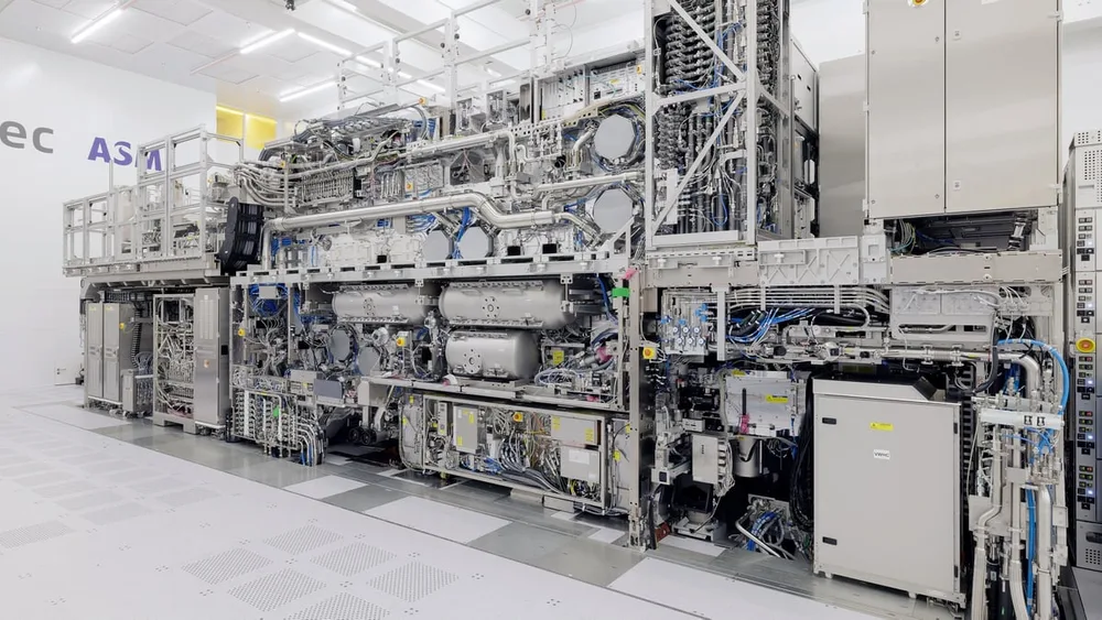
The technical reality of the EUV bottleneck
For those not deep in the semiconductor weeds, the move to larger masks isn't just a "size update." It's about how many chips can be exposed per flash. By increasing the mask size, ASML is allowing these giants to push more silicon through the pipeline without increasing the number of passes. This is a direct play to lower the cost-per-die as we move toward 2nm and beyond.
However, this creates a massive barrier for anyone trying to build a competing lithography stack from scratch. When the industry standard shifts toward a specific mask size and machine specification, every other part of the supply chain—from the photoresist chemicals to the pellicles—has to align.
Breaking the dependency loop
Huawei is trying to orchestrate a workaround via Yuliangsheng and a network of domestic suppliers. The goal here isn't just to "copy" a machine, but to build a parallel ecosystem that doesn't rely on Dutch IP.
The struggle is that lithography isn't just about the machine; it's about the precision of the light source and the materials. If you can't match the throughput of the newest EUV iterations, you're fighting a losing battle on yield. Even if they manage to get a machine running, the gap in "wafers per hour" is where the real war is won.
My take on the hardware lock-in
I see this as a classic vendor lock-in scenario on a planetary scale. When your entire manufacturing process is optimized for a specific hardware spec (like these larger photomasks), switching costs become astronomical. You aren't just changing a tool; you're redesigning your entire fab layout and process flow.
If I were analyzing this from a deployment perspective, the risk isn't just "not having the machine," but having a machine that is 40% slower than the competition. In the chip world, 40% is an eternity. It's the difference between dominating the mobile market and being a niche player.
The real question is whether a fragmented supply chain can ever catch up to a vertically integrated one. If Huawei and Yuliangsheng can't hit those throughput numbers, they'll be stuck in a cycle of playing catch-up while the big three accelerate away.